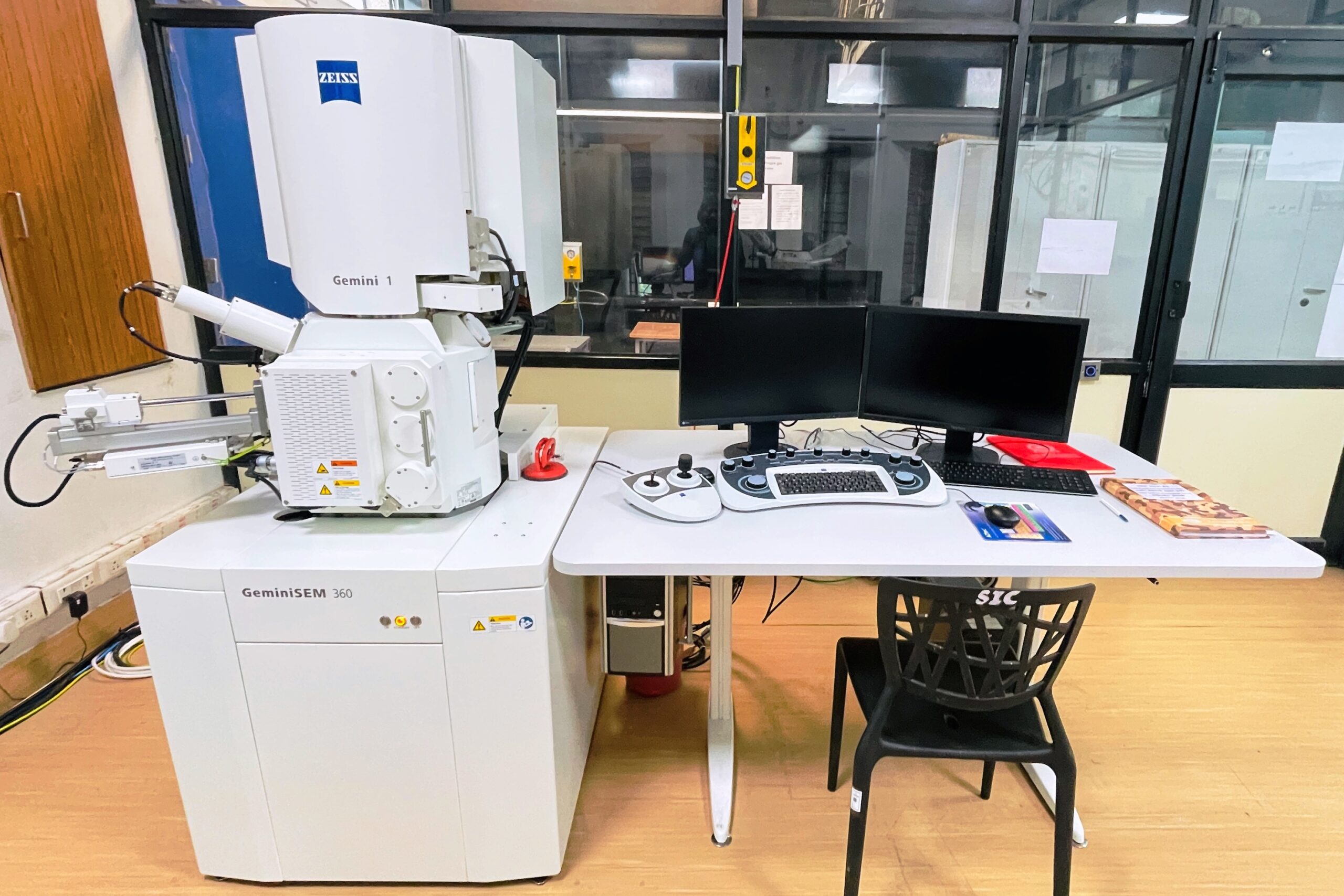
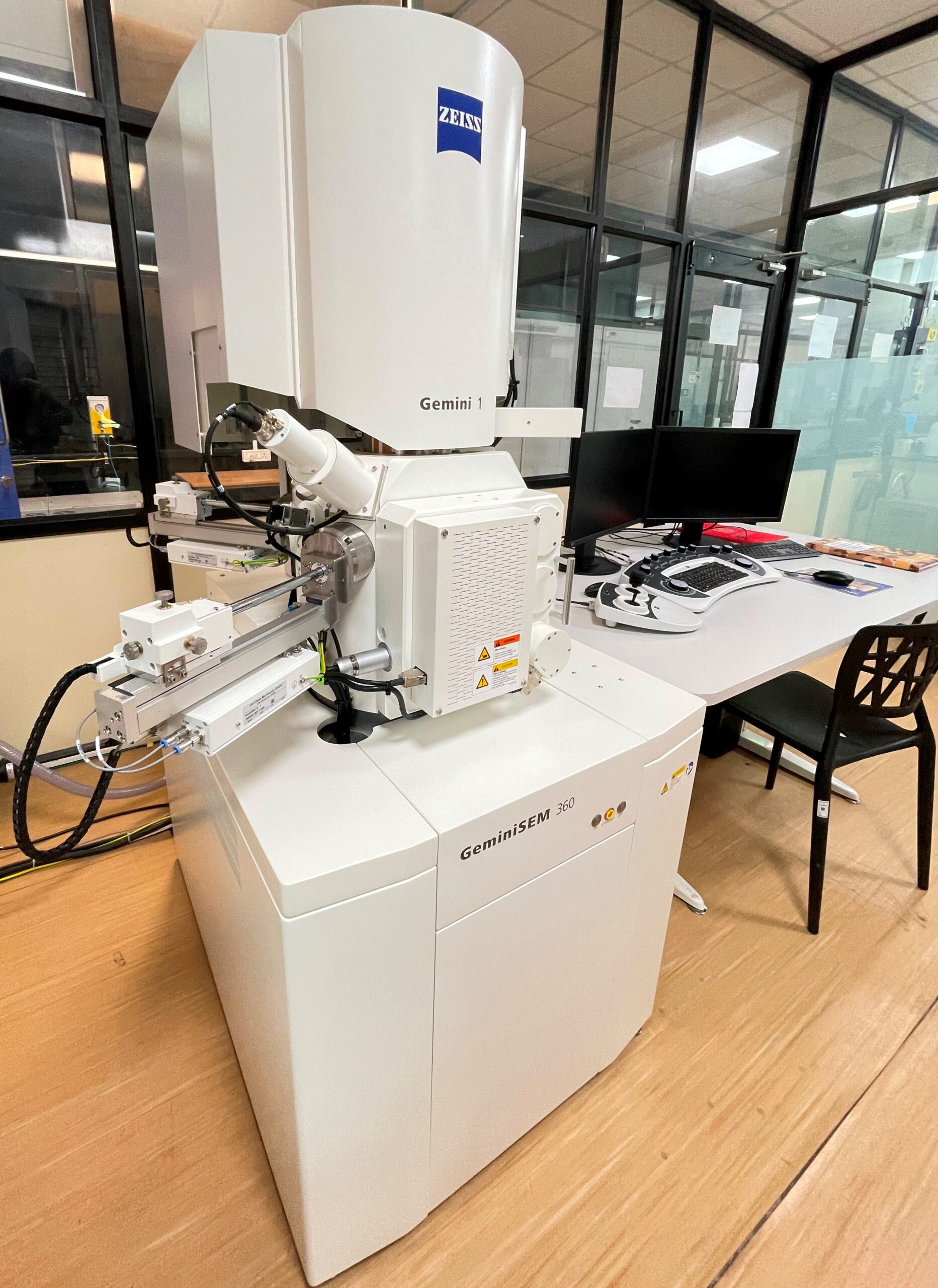
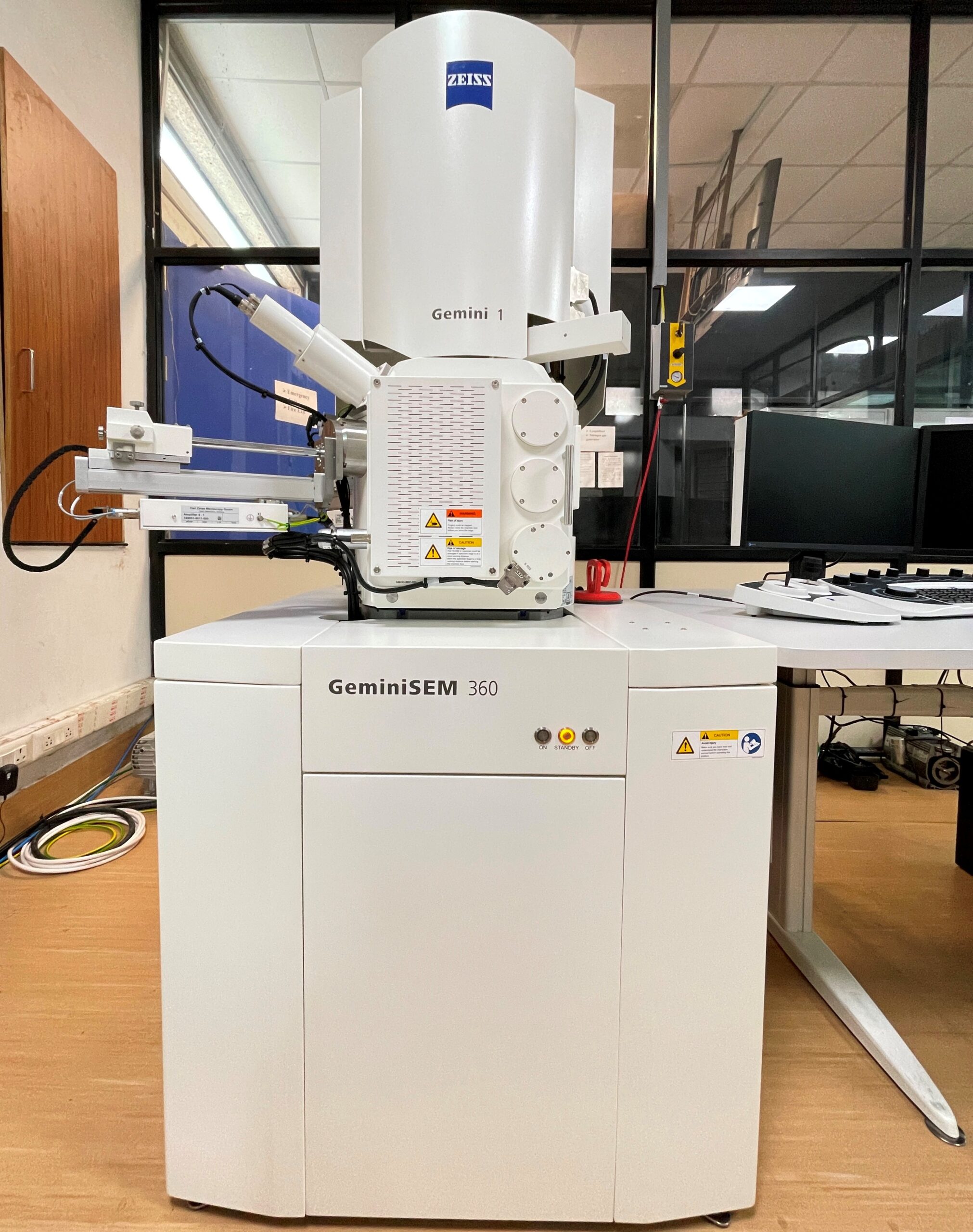
Model
ZEISS GeminiSEM 360(Germany)
Features
GEMINI Technology with high efficiency in-lens detector and no magnetic field at specimen level.
Superb resolution and image quality at high and low operating voltages.
Extremely wide operating voltage range from 0.02-30kV.
Designed-in ease of use with minimal adjustments required when changing operating conditions.
Short analytical working distance of 8.5 mm for simultaneous high resolution imaging and X-ray analysis.
High probe current (up to 100 nA) with high stability (better than 0.2%/h) for precise analytical results.
Multi-User friendly with Windows® based Smart SEM control software.
Backscattered Electron (BSE/BSD) Detector:
The BSE detector in the Gemini SEM360 is designed to capture high-energy electrons that are reflected or backscattered from the sample. BSE imaging provides contrast based on the atomic number of elements, making it useful for compositional analysis. Heavier elements appear brighter, allowing for differentiation between different materials within the sample.
Scanning Transmission Electron Microscopy (sTEM) Detector:
The sTEM detector in the Gemini SEM360 enables transmission imaging at nanoscale resolution. This detector is particularly valuable for analyzing thin samples, such as foils or cross-sections, where it provides detailed information on the internal structure of the material. The sTEM mode allows for atomic-level imaging and analysis, making it indispensable for research in materials science, nanotechnology, and semiconductor development.
Applications
1. High-Resolution Imaging and Surface Analysis
- Surface Morphology: The SE1 and InLens detectors provide high-resolution imaging of surface features. SE1 is excellent for topographical contrast, making it ideal for studying surface textures, cracks, and other fine details on materials like metals, polymers, and biological samples.
- Nanostructure Analysis: The high resolution offered by InLens, combined with SE1, allows for detailed imaging of nanostructures such as nanoparticles, nanowires, and thin films, crucial for research in nanotechnology and material science.
2. Elemental Composition and Mapping
- Phase Identification: EDX enables the identification and mapping of different phases within a material. This is particularly useful in metallurgy, ceramics, and composites, where distinct phases need to be characterized.
- Contaminant Detection: EDX can detect and quantify impurities or unwanted elements in materials, which is essential in failure analysis, quality control, and environmental studies.
- Chemical Composition Analysis: EDX, combined with sTEM mode, provides detailed elemental analysis and mapping, even in thin or small samples, enhancing the understanding of complex materials.
3. Transmission Electron Microscopy (sTEM)
- Thin Film Analysis: sTEM allows for the study of thin films at high resolution, providing information on the film’s structure, thickness, and composition. This is critical in the semiconductor industry and for the development of advanced materials.
- Cross-Sectional Imaging: sTEM is used to obtain cross-sectional images of samples, allowing for the analysis of layered structures, interfaces, and defects within materials like semiconductors, MEMS/NEMS devices, and composite materials.
- Nanoparticle Analysis: sTEM can be used to analyze the internal structure and composition of nanoparticles, providing insights into their properties and potential applications in catalysis, medicine, and materials science.
4. Material Contrast and Composition Imaging
- Atomic Number Contrast (BSD): The BSD provides atomic number contrast, allowing for the differentiation of materials with different compositions. This is particularly useful for studying composites, geological samples, and multiphase materials.
- Microstructural Analysis: BSD is used to reveal microstructural features such as grain boundaries, inclusions, and phase distributions in materials like metals and ceramics, aiding in understanding material properties and behavior.
5. Advanced Research and Development
- Catalysis Research: The combination of high-resolution imaging and elemental analysis is ideal for studying catalysts, particularly in terms of surface structure, active sites, and material composition at the nanoscale.
- Material Science Research: The Gemini 360 SEM is used to investigate the microstructure, composition, and properties of advanced materials, including metals, ceramics, polymers, and nanocomposites. It aids in developing new materials with enhanced properties.
- Semiconductor and Electronics: sTEM and EDX are crucial for analyzing semiconductor devices, including thin films, layered structures, and detecting defects or impurities that could affect performance.
6. Biological and Medical Applications
- Cell and Tissue Imaging: The SE1 and InLens detectors can be used to image the surface morphology of biological samples, such as cells and tissues, without the need for extensive preparation, preserving the natural structure.
- Biomaterial Analysis: EDX and sTEM are useful for studying the composition and structure of biomaterials, such as implants, to ensure biocompatibility and understand their interaction with biological tissues.
- Drug Delivery Research: sTEM can be used to analyze nanoparticles used in drug delivery systems, providing insights into their structure, composition, and effectiveness.
7. Geology and Mineralogy
- Mineral Identification and Mapping: EDX and BSD are used to identify and map the composition of minerals in geological samples, providing insights into their formation, history, and potential applications.
- Textural and Structural Analysis: SE1 and InLens detectors help analyze the texture and structure of geological samples, aiding in the understanding of geological processes and resource exploration.
8. Forensic Science
- Trace Evidence Analysis: The high-resolution imaging and elemental analysis capabilities of the Gemini 360 SEM make it ideal for analyzing trace evidence, such as gunshot residues, paint chips, or fibers, in forensic investigations.
- Failure Analysis: sTEM and EDX can be used to study material failures, such as fractures or corrosion, by analyzing the composition and structure of the affected areas.
9. Archaeology and Art Conservation
- Artifact Analysis: The Gemini 360 SEM is used to analyze the composition and surface details of artifacts, helping in authentication, preservation, and understanding ancient manufacturing techniques.
- Conservation of Artworks: EDX and BSD are employed to study the composition of pigments, metals, and other materials in artworks, guiding conservation and restoration efforts.
Handled By Mr. Sagar Patail
sagarpatail@iiti.ac.in